Technology
Nvidia Partner Invests 4 Billion in Indiana
It is expected that the South Korean memory chip manufacturer will establish a state-of-the-art packaging factory in West Lafayette and create up to 1,000 jobs.
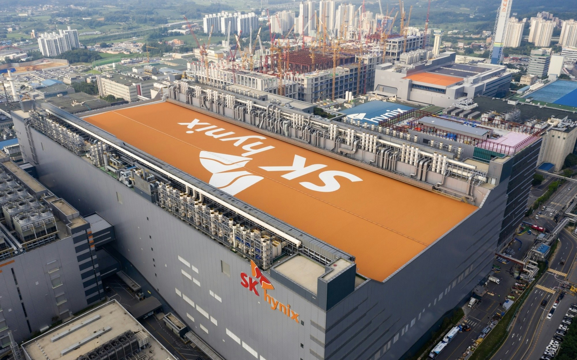
SK Hynix, the South Korean Memory Chip Specialist, Plans Monumental Investment to Power the Heartland of the USA with Cutting-Edge Technology. About 4 Billion Dollars are to Flow into West Lafayette, Indiana, to Build a State-of-the-Art Chip Packaging Facility that Could Create Up to 1,000 Jobs. This Strategic Decision Marks a Significant Step in the Biden Administration's Efforts to Once Again Make the United States a Global Power in the Semiconductor Industry.
Proximity to Purdue University, one of the leading institutions in the USA in the field of semiconductor and microelectronics engineering, grants SK Hynix access to a pool of highly qualified engineers. State and federal tax incentives, as well as other forms of support, are expected to contribute to the project's financing. Operational commencement is planned for the year 2028, with a final decision from the SK Hynix board imminent.
SK Hynix, Known as One of the World's Largest Chip Manufacturers, Has Gained Significant Importance Particularly Due to the Recent AI Boom. The Company Leads the Market for "High-Bandwidth Memory" (HBM) and Serves as an Exclusive Partner for Nvidia's Most Advanced Graphics Processing Units. This Partnership Enables Accelerated Data Processing Essential for Generative AI Tools Like OpenAI's ChatGPT.
The new facility in West Lafayette would represent the first major HBM packaging factory in the USA, thus marking a significant change for an industry whose production has so far taken place almost exclusively in Asia. Advanced chip packaging is a critical aspect of the US Chips Act of the Biden administration, which provides at least around 3 billion dollars for the expansion of domestic production.
The ability to anchor at least parts of the production chain for such sought-after technologies in the USA would be a significant breakthrough. HBM is a cutting-edge technology that utilizes advanced packaging techniques and materials to stack and fuse individual DRAM chips together, dramatically increasing data processing capacity. SK Hynix's HBM3E generation can process the data volume of 230 HD movies in one second.
The decision for Indiana was also due to the planned facility of SkyWater Technology in West Lafayette, a project worth 1.8 billion dollars, announced in 2022. The construction costs for the SK Hynix packaging facility in the USA are estimated to be 30% to 35% higher than for a comparable facility in South Korea. It is expected that funding from the US government will offset some of these additional costs.
This investment is part of the commitment from the SK conglomerate to invest about 30 billion dollars in the USA over the coming years, with half of these investments intended for the semiconductor sector. This underscores the company's dedication to lead not only in the semiconductor industry but also in the fields of electric vehicle batteries and biotechnology.